


Pressure is gradually becoming important in manufacturing semiconductors due to semiconductor’s miniaturization. Under this circumstance, manufacturing equipment and material manufacturers as well as semiconductor manufacturers have begun to use PRESCALE in various applications such as “measuring polishing pressure in a Chemical Mechanical Polishing (CMP) equipment” ”checking pressure distribution of laminating press in manufacturing an Electrostatic chuck or a Ceramic heater” or ”measuring pressure distribution of a Molding machine” etc.
In this page, we will introduce some applications along the semiconductor manufacturing process. Of course, there are a lot of applications besides the followings, so if you want to measure surface pressure easily and at low cost, please feel free to request our samples.
Process
Front-end process (Wafer processing operation)
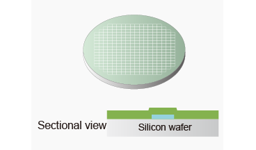
1. Purchase of silicon wafers

A silicon wafer is a disc-shaped piece of high-purity silicon. Wafer size is generally 200mm/300mm.
Some semiconductor manufacturers are now considering 450mm as a next generation standard.
2. Cleaning process

Since there are various kinds of dust or metal ions on the wafer immediately after purchase, they are removed with high-purity acid or alkali chemicals.
3. Film deposition process

The insulating film and conductive film used for semiconductors are deposited on a wafer.
4. Photolithography process

A circuit pattern is drawn (transferred) on a wafer with a reticle.
5. Ion implantation process

Some impurities such as phosphorus and boron which determine the electrical characteristics (P, N type) of semiconductors are implanted into the wafer.
6. Etching process

The deposited films are removed excepting films under the pattern of the regist.
7. Deposition process
A wafer is covered with insulation films which separate wirings by each layer.
8. Chemical-mechanical polishing process

A wafer surface is polished and flattened in order to facilitate subsequent processes.
Back-end process (Assembly process)
9. Pasting surface protection tape

A protection tape is attached on the circuit surface or a wafer in order to protect a circuit during back grinding.
10. Backgrinding process

The back side of a wafer is grinded to be thin overall.
11. Pasting dicing tape

A dicing tape is applied to a wafer in order to fix it.
12. Dicing process

A wafer is cut into many tiny tips.
13. Mounting process

A tip is mounted onto a metal lead frame.
14. Bonding (wire bonding) process

A tip is connected to electrodes in the lead frame with gold wires.
15. Molding process

A tip is molded to be a package with a resinous encapsulant.
16. Marking process

The product name or manufacturer name is marked on the package.
17. Inspecting process

Tips inspected to be good products are shipped.
Semiconductor substrates
Rigid substrates

Flexible substrates

Transistors

